A More RealisticAdder
All our designs so far suffer a major reality problem; they do not account for signal delays. In real systems it takes time for the information to propagate through the gates of a device. Verilog allows us to annotate our models to include timing information. In fact Verilog is capable of very sophisticated timing models including max, min, and average timings for all transitions. We don't need anything that complex but we should include some delays tom make our model more physical.
The simplest block in our system is the full adder. It uses logic expressions to represent the behavior of gates. A full timing model would require us to replace the logic expressions with good models of the individual gates. A simpler path is just to tell Verilog the maximum length of time it takes any change to propagate through the expressions.
Here are the relevant lines from fadd.v:-
 assign cout = (a & b) | (a & cin) | (b & cin);
 assign q = a ^ b ^ cin;
Assuming that we have a 3-input OR each of these is two gates deep; one AND & one OR for cout, two XORs for q. From the data sheets we find that the XOR has a delay of 20nS while both the AND & OR have a delay of 15nS (assuming the use of 74HC series devies). Thus we add delay times to the full adder to get
//	Full-adder with propagation delays added.
//
`timescale 1ns/100ps
module fadd(a, b, cin, q, cout); output q, cout; input a, b, cin; assign #30 cout = (a & b) | (a & cin) | (b & cin); assign #40 q = a ^ b ^ cin; endmodule // counter |
We have two changes. First is the introduction of a timescale (which will have to be added to all our files!) and then there are the actual delays on the assign lines. Because of the timescale these are in units of nS so that we have specified a 30nS delay for the cout signal.
The process is the same for the flip-flop and register. The 7474 data sheet tells us we have a propagation delay from clock or set/reset to Q of 20nS (at 25C) and the 74194 has a delay of 14nS.
Putting these delays in, not surprisingly, seriously alters the behavior of our adder!
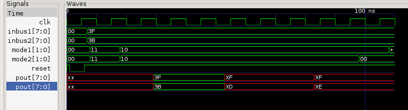
A very little thought shows us one major reason; our clock is way too fast. We have delays at the 20nS level and a clock period of 10nS (100MHz). Slowing the clock to 10MHz we get exactly the same thing! The fact that the lower nibbles of the registers are remaining defined suggests that the problem is with the feed-round and may have to do with the carry flip-flop. I added the flip-flop signals to get
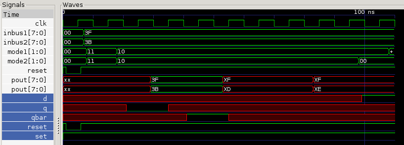
Here we see that the flip-flop is never being reset! The reset is not low for long enough for it to take effect. Let's lengthen the reset from 5nS to 50nS.I will lengthen all the times by the same factor of 10. That makes a major improvement. Register B is now fine but there is still a problem with the serial input to register A since the top nibble is still not working..
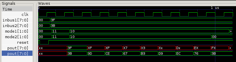
The serial input to register A comes from the sum output of the adder so let's look at the adder.